Department
of Electronics. University of Valladolid
Atomistic
Process Simulation at e-UVA
Conference presentations about the
simulation technique and its capabilities:
·
IEEE
International Electron Device Meeting (IEDM 2007). Washington DC, USA
Current Capabilities and Future Prospects
of Atomistic Process Simulation pdf
(1.7 MB)
·
Simulation
of Semiconductor Processes and Devices 2007 (SISPAD 2007)
Atomistic modeling of defect diffusion in
SiGe. pdf
(700 KB)
·
Presentation in Crolles, France, April 2005.
Predictive Front-End Process Simulation: The kinetic Monte Carlo
Approach pdf (2.2MB)
·
Spanish
Conference on Electron Devices 2003 (CDE03). Calella, Spain.
Simulación Atomística de Procesos
en Microelectrónica. pdf
(2.2MB)
·
2nd
Int. Conf. on Computational Nanoscience and Nanotechnology, 2002 (ICNN2002).
Introducing
·
32th
European Solid-State Device Research Conference, 2002 (ESSDERC 2002). Firenze, Italy.
Exploring Methods for Adequate Simulation of Sub-100nm Devices. pdf (724KB)
·
Int.
Conf. on Simulation of Semiconductor Processes and Devices, 2001 (SISPAD 2001).
Athens, Greece.
Atomistic Front-End Process Modeling: A Powerful Tool for Deep-Submicron
Device Fabrication. pdf (4.4 MB)
·
Mat.
Res. Soc. Spring Meeting 2000. San Francisco, CA.
Symposium: Si Front-End Processing – Physics and Technology of Dopant-Defect
Interactions II.
Atomistic Process Modeling: An Accurate and Straightforward Approach for
Complex Processing Scenarios. pdf (3.2 MB)
·
Challenges
in Predictive Process Simulation 2000 (ChIPPS 2000). Wandlitz, Germany.
Building a bridge between ab initio calculations and process simulation. pdf (1MB)
·
European
Mat. Res. Soc. Spring Meeting 1999. Strasbourg, France.
Kinetic Monte Carlo Simulation: an Accurate Bridge Between Ab-Initio
Calculations and Standard Process Experimental Data. pdf (3.4 MB)
·
Mat.
Res. Soc. Spring Meeting 1998. San Francisco, CA.
Symposium: Silicon Front-End Technology - Materials Processing and Modeling.
Atomistic modeling of point and extended defects in crystalline materials. pdf (1.6MB)
|
Simulation
of a |
|
|
|
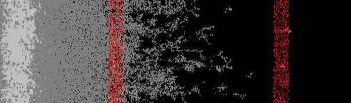
Time-evolution
observed in the movie: AP annealing occurs during rump-up. V-clusters
survive only near the surface while I-clusters and {311}’s experience ripening.
Some small I-clusters, having “magic number” survive for a while. The total
Interstitial concentration in the sample after V-cluster dissolution is in
good agreement with +1 model (~5e13 cm-2). Boron in the shallowest spike exhibits a
noticeable clustering whereas the deepest one suffers a high diffusion (TED)
and almost no clustering. When {311}’s disappear TED finishes and only a slow
BIC dissolution is observed. |